In Part 7, we looked at Micron’s outlook that the memory shortage could last until 2028
🔗 Link - https://blog.naver.com/rottensweetpotato/224432164780
On October 14, Ahn Hyun, President and head of development at SK hynix, presented a post-HBM vision at SEDEX 2026
 SK hynix logo
The bottleneck of moving data between memory tiers
Ahn explained that AI inference demand grows by task complexity times context length times number of requests On that basis, he projected that the performance scale of AI infrastructure in 2030 will be about 19–20 times that of 2026
The multiple was reported as 19 times or 20 times depending on the outlet
The bottleneck he pointed to is moving data between memory tiers
Previously, the bottleneck was transfer between compute units and memory His diagnosis is that now, data split across HBM, DRAM, and SSDs takes time to move between tiers
He cited the KV cache as the cause It’s the space where AI stores information about tokens it has already read so it can reuse it, and it grows as context gets longer
The memory hierarchy, revisited
In Part 2, we looked at the difference between DRAM and SRAM
SRAM is fast but expensive and small, so it’s used as cache inside chips DRAM is slower but larger and cheaper
🔗 Link - https://blog.naver.com/rottensweetpotato/224350430384
| Position | Technology | SK hynix announcement |
|---|---|---|
| Inside compute units | SRAM | The fastest memory |
| Between SRAM and HBM | New tier | 3D-stacked DRAM |
| Next to the GPU | HBM | Expanding custom HBM |
| Between HBM and SSD | HBF | Target of 10x capacity |
| Across servers | CXL memory | Developing pooled memory |
3D-stacked DRAM
 Concept shot of DRAM layers stacked vertically on a GPU chip and connected by tiny through-electrodes — Source: concept shot, self-generated with agy
Saying “the fastest memory in existence is SRAM,” Ahn said a new tier is needed between SRAM and HBM What he put forward for that slot is 3D-stacked DRAM
It stacks DRAM directly on top of compute chips such as GPUs and NPUs and connects them with TSVs (through-silicon vias) HBM sits next to the compute chip, but 3D-stacked DRAM is stacked on top of it, shortening the data transfer distance
According to reports, the goal is to increase the number of input/output paths (I/O) by tens of times compared with HBM He said the problem of heat concentrating when chips are stacked would be solved with advanced packaging
No concrete figures such as launch timing or capacity were announced
HBF and other memory technologies
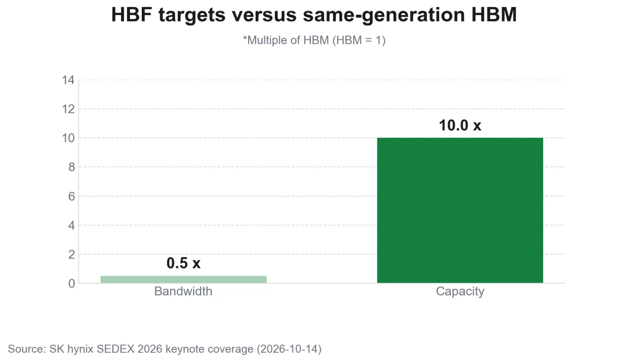 Bar chart of HBF targets of 0.5x bandwidth and 10x capacity versus same-generation HBM — Source: self-rendered based on reports of the SK hynix keynote
HBF (High Bandwidth Flash) is the stacked NAND memory covered in Part 6 SK hynix set targets of half the bandwidth and about 10 times the capacity of same-generation HBM
🔗 Link - https://blog.naver.com/rottensweetpotato/224386687366
The explanation is that NAND has a short write lifespan but suits work that reads the same data repeatedly, such as AI inference
It released draft spec 0.7 at OCP in July It was reported to be working with Sandisk and others toward a final spec in January 2027
🧩 Other development items
- Custom HBM: putting customer functions into HBM’s base die; expected over the long term to grow larger in share than standard HBM
- CXL pooled memory: a structure in which multiple servers share memory resources
- Storage Next: SSD technology that improves I/O processing performance 4–8 times over existing levels
The two Korean companies’ approaches
At Hot Chips in August, Samsung Electronics presented a direction of putting compute functions into HBM’s base die SK hynix emphasized subdividing the tiers and adding new memory between them
Both approaches try to keep data close to the compute units Ahn said memory is Korea’s best industry and now is a golden opportunity
Sources
- [Financial News] SK hynix President Ahn Hyun’s SEDEX 2026 keynote (2026-10-14, new tier between SRAM and HBM, 20 times)
- [iNews24] Solving the AI memory bottleneck with 3D-stacked DRAM and HBF (2026-10-14, 19 times, HBF spec schedule, Storage Next)
- [Herald Economy] HBM alone can’t meet memory demand, HBF and 3D-stacked DRAM in development (2026-10-14)
- [eToday] AI bottleneck must be solved by optimizing the entire memory hierarchy (2026-10-14)
- [iNews24] Hot Chips 2026: Samsung makes HBM smarter vs. SK makes it taller (2026-08, Samsung base die compute)
- Basis for figures: the original SK hynix newsroom post was not checked; values are those consistent across multiple outlets’ reports